Synchronous counter:This is the simplest synchronous sequential circuit.
How can we design a modulo 6 counter ?
We know a mod 6 counter counts the sequence (0, 1, 2, 3, 4, 5, 0, 1, …). It has 6 counts or 6 states which starts with 0 and then count 1, 2, 3, 4, 5 and then loops back to 0 and continues. This is a binary counter. We need log2(number of states) flip flops to design this counter which is equal to 3 in this case.
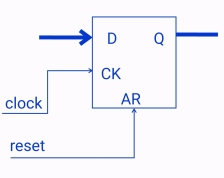
So let us put the 3 flips flops here as shown in figure. The clocks and the asynchronous reset to the 3 flops are tied together. There are 3 Qs (Q2, Q1 and Q0) as output and 3 Ds (D2, D1 and D0) as inputs. Assume at power on ,the output Q becomes (000). When the clock comes we should get (001) at Q.
So how to make the output 001 ?
As we know when the clock comes, as far as registers are concerned, whatever at D is transferred to Q. So it is enough that if we can make ready ‘001’ at the input D, then upon the clock edge, this D(001 ) is transferred to the output Q. In the next clock ‘010’ should be ready at D and so on.
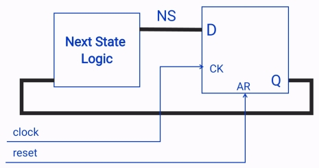
So it is enough that if we put a combinational circuit(next state logic or NSL) before the input D of flif flops and feedback the present count to the input of that circuit (NSL). So we design the circuit such that
given 000 –> should give 001
given 001 –> should give 010 and so on.
So this is the structure of a synchronous counter. We have flip flops and we call this ouput Q as Present State(of the FFs) and it goes to a combinational circuit and the output of comb circuit is called the Next State (NS) because upon the clock, the Next State becomes the Present State.
We call this combinational circuit as Next State Logic because it is a logic /comb circuit which decode the NextState(NS) from the Present State(PS).
Now how to design this Next State Logic ?
In order to design the NS Logic, we need to write the Truth Table in terms of the input (Present State) and Next State as shown below.
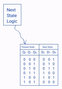
The Present State has 3 inputs (Q2, Q1, Q0) and the Next State has 3 outputs(D2, D1, D0). The moment we write the Truth Table, we have to look the D2 separately, D1 separately and D0 seperatlely and pick out the ‘1’ s in colomns of D2, D1 and D0 and minimize it using K map and come out with a SOP (sum of products) equation in terms of Q2, Q1 and Q0. So ultimately you will get 3 boolean equations for Ds (D2, D1 and D0).
ie Di =Fi (Q2, Q1, Q0) or
D2= F2(Q2, Q1, Q0); D1= F1(Q2, Q1, Q0); D0= F0(Q2, Q1, Q0);
ie NS = function (Present State);
It is enough that if you describe the Truth table in terms of an HDL(VHDL or Verilog) in a high level design, you will get this design.
Reference: NPTEL Lecture series on Digital System design with PLDs and FPGAs by Kuruvilla Varghese, DESE, IISc Bangalore