Setup and Hold Timings with skew in clock path

setup_hold_with_clock_skewIn the last post we have discussed the setup and hold timings when there is a skew in the data path. In this section we will discuss the case when there is a skew in the clock path.

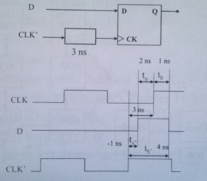
As shown in the diagram there is a 3 ns skew in the clock path. Assume that there is no skew in data path. We have a pin at CLK’ that suffers a delay of 3 ns before it reaching the CK port of the particular flip flop. We would like to know the relation of the data setup and hold time at D with respect to CLK’ where we have control.

The original clock(CLK) is shown and has a setup time of 2 ns and hold time of 1 ns with respect to D. The new reference clock CLK’ is appearing earlier to CLK by 3 ns.  If you refer to the waveforms you can see that, the data at D is setting up after the active edge of CLK’. So the setup time which was earlier 2ns is now -1 ns (2ns -3ns) which is negative. Now for the hold time, the data has to be stable for an additional 3 ns after the active edge of CLK’ resulting a hold time of 4 ns.

So this means that if there is a skew in the clock path, the setup time is reduced and the hold time is increased, both by the delay in the clock path. In this case the setup time can be negative which means that with respect to CLK’, the data is setup after the active clock edge.

Point to note:

  • When there is a delay ‘t’ in the path to clock input, the setup time with respect to new reference point CLK’ is decreased by t and hold time is increased by t.
  • In this case the setup time can take a negative value. A setup time of -t means that at point CLK’ the data at D can be setup ‘t’ time after the active clock edge.
  • Setup time is defined as time before clock, the data has to be setup. So for setup time positive value is going backward from the clock edge and negative value means it is forward from the clock. For hold time, the reverse case applies.

Reference: NPTEL Lecture series on Digital System design with PLDs and FPGAs by Kuruvilla Varghese, DESE, IISc Bangalore
Setup and Hold Timings with skew in clock path

Setup and Hold Timings with skew in data path

setup_hold_with_data_skewWe know that for a flip flop, the setup time and the hold time is specified at the input D as shown in the diagram. The timing parameters states that, with respect to the active clock(CLK) edge, there is a setup time (ts = 2ns) before which the data has to be setup and there is a hold time (th = 1ns) for which the data has to be held some time after the clock edge.

Here in this waveform, the data is changing from 0 to 1, 2 ns (ts) before the active clock edge and remain high for 2 ns up to the clock edge and 1 ns more after the clock edge and then it changes.

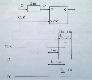
But many at a times we may take the input at a pin D’ on a chip, like a wire is going from a pin through a buffer and reaches at D. So there could be additional delays in the data path. Here in this case point D’ incur a delay of 2 ns w.r.t D, meaning that when you give a data at D’, it appears at D after 2 ns delay. When you supply a clock (assume CLK has no delay) we would like to know what is the setup time and hold time w.r.t the point D’, because we have control over this point only, we are supplying data from outside at this point and we are not worried about the setup and hold time at the point D since that doesn’t help us because there is an additional 2 ns delay.

what is the new setup time at D’ ?

With respect to CLK, the setup time has increased because the data at D’ has to be setup 4 ns (old 2ns(ts) + 2ns data path delay) before the active clock edge. So the data path delay 2 ns is added to the setup time and setup time has increased.

What is the new hold time at D’?

Hold time is 1 ns towards left of the active clock edge. Remember Setup time is defined as the time before the active clock edge, the data has to setup and the Hold time is defined as the time for which the data has to to be held after the active clock edge. But here in this case, the data is removed before the active clock edge (normally we remove data after the active clock edge) and so the hold time become -ve and is -1 ns (old 1ns (th) – 2 ns data path delay). When the hold time become -ve in the opposite direction, it means that you can remove the data at D’ even before the active clock edge.

Points to note

  • When there is a delay ‘t’ in the path to D input, the setup time w.r.t new reference point D’ is increased by t and hold time is decreased by t.
  • In this case hold time can take a -ve value. A hold time of -t means at point D’, the data can be removed or changed ‘t’ time before the active clock edge

Reference: NPTEL Lecture series on Digital System design with PLDs and FPGAs by Kuruvilla Varghese, DESE, IISc Bangalore

Setup and Hold Timings with skew in data path

Digital Design: Major Constituents

Suppose somebody asked us to design a Multiplier, what should we focus on?

Some may say that we should focus on Low Power, Low Area, working at a certain frequency etc.

  • Function/Logic

The function or the logic is the primary part to consider while designing any system while power, area, frequency and all come later. What is the use if we get wrong results out of a design which is power wise or area wise or timing wise very perfect. In every data sheets of IC, the first thing stated is the function of the IC and that shows that function has priority over the others.

Digital Design: Major Constituents

Learning vs Design

  • Learning : Bottom up

Transistor => Gates => Combinational => Sequential => Computing Blocks => System

  • Design : Top Down

Processor => ALU, Register,….

ALU => Adder, subtractor, ….

Adder=> Gates => Transistors

In Learning we always go bottom up starting from the smallest piece to the complex one. Normally we start with transistors (nMOS, pMOS, cMOS etc). Then we will see how to build the logic gates (like AND, NAND, XOR etc) based on these transistors.By using gates we will learn building the combinational circuits (like Adders, subtractors etc)  and sequential circuits (like Controllers, Data Path or Registers with combinational circuits). Then we will see how to interconnect all these elements to build a complete system.

When we Design, it is the opposite process we adopt, ie we choose Top Down. Suppose we are designing a Microprocessor, we break this into pieces like ALU, Registers, Program Counter, Stack Pointer and so on.Then we take one of the piece say ALU and break down this into Adder, Subtractor and so on. Then we take the Adder which is designed in terms of XOR, AND and OR gates. Then ultimately these gates are converted into CMOS Transistors.

Reference: NPTEL Lecture series on Digital System design with PLDs and FPGAs by Kuruvilla Varghese, DESE, IISc Bangalore

Learning vs Design

Digital Sytem Design Overview

  • Specification to Implementation

The system may be a counter or an ALU or a Microprocessor or a SOC. Having only the knowledge of specification and the domain how will you go and implement the design.

  • Algorithm to Architecture (Front end Design)

Very specific objective. For eg, you have a signal processing algorithm for a filter, how do you design an architecture for that filter and in VLSI it is called the Front End Design. That is you have the specification and from the specification you go all the way to the logic design – ie design in terms of gates and flip flops.

Back End Design : In this design, it takes these gates and flip flops all the way to transistors and the mask required for the chip or the IC manufacturing.

  • Partitioning, Design of blocks, Timing Analysis

Partition the system into pieces/blocks and take each block and design in detail meeting the specification and at least you have to do a timing analysis of each block to be able to work. That is at least make it work in a functional way and it should meet the basic delay requirements.

  • Advanced Digital Design: Top-down Design, Data Path, Controllers, Timing ..

Top Down Design or Hierarchical Design: In undergraduate courses we have done our designs like Full Adders in terms of  known gates (AND,XOR etc)  and Counters using  gates and Flip Flops. We started our design with Truth Table and Boolean Equations, Minimizing and implement it with gates and Flip Flops. But when you design a complex system( like a CPU ) we will not be able to do the design at the gates and Flip Flops level. We have to use the known combinational blocks like the encoders/decoders, multiplexers/demultiplexers, adders/subtractors  and sequential blocks like Registers, Counters and so on.

Data Path talks about the basic computation (ie the circuit where all computation happens). Controller is the one which moves or controls the data movement within the Data Path and there could be a single controller or multiple controllers in a system.

Timing: After the design of both the Data Path and Controllers, we are definitely concerned about the timing, that is How to meet the timing requirement parts of the specification.We have different parts of the digital systems working on different clocks or there may be part of the system working on one clock and the system may receive some manual input from a limit switch or a keyboard and unless these asynchronous inputs are handled carefully by synchronizing  to the receiving domain, these inputs may not be registered properly in the receiving clock domain.This is called the synchronisation aspect of the design

Reference: NPTEL Lecture series on Digital System design with PLDs and FPGAs by Kuruvilla Varghese, DESE, IISc Bangalore

Digital Sytem Design Overview